Technology for the 21st Elevator Century
Dec 1, 2016
The science behind a product touting full door-area protection for passengers, freight and the door itself
This paper was presented at  Madrid 2016, the International Congress on Vertical Transportation Technologies, and first published in IAEE book Elevator Technology 21, edited by A. Lustig. It is a reprint with permission from the International Association of Elevator Engineers
  (website: www.elevcon.com).
The decades-old light curtains used to safeguard elevator doors are about to be disused thanks to new time-of-flight (TOF) technology. Thus, the transition from 2D to 3D is enabled by the optical touch-free full-3D sensor TOFgard. This little (40 times smaller than light curtains), EN 81-20-compliant sensor offers the safeguarding function across both the cabin and landing door closing edges and a genuine full door-area protection for passengers, freight and the door itself. It reduces accidents while significantly increasing the functionality by intelligently monitoring the complete 3D area. The 3D technology can also count people, which is very useful in connection with destination call control.
In 1886, Heinrich Hertz discovered that electromagnetic waves are reflected from metallic objects. However, it took almost 20 years (until 1904) for German engineer Christian Hülsmeyer to present the first functional radar system. He could detect big objects (like ships) up to a distance of 3 km. Hülsmeyer used electromagnetic waves with a wavelength of 50 cm, which have a carrier frequency of approximately 300 MHz. Since then, the radar principle has been developed so objects’ distance, velocity and, roughly, size can be measured. However, due to the relatively long wavelength, spacial resolution is very poor.
Thus, intense R&D took place to reduce the wavelength and thus increase the spacial resolution. The current limit is a carrier frequency in the region of 100 GHz that represents a wavelength of approximately 1.5 mm. However, the spacial resolution is still very poor, due to the propagation of electromagnetic waves with a wavelength longer than a few micrometers that can only be guided with very big antennae. Thus, the research for radar systems using wavelengths in the micrometer range or less was ongoing. Electromagnetic waves in this wavelength region are commonly termed “light.” Thus, the scientific society changed the name from “radar” to “lidar” (“light detection and ranging”). The propagation of light in space can easily be controlled by lenses and mirrors, which serve as antennae for these kind of electromagnetic waves. Lidar originated in the 1960s and is used to measure aerosols (e.g., for weather forecasting). Typically, lidar systems are big installations and need scanners to produce images, because lidar measures just the distance at one spot.
In 1985, when your author started research in the 3D imaging field, the term “TOF” did not exist, and imaging was not even a topic. However, his fascination was to provide something that could become a 3D camera where every pixel has the capability to measure the distance to its individual object point. Also during that time, with lidar concepts, a distance resolution in the range of 1 m was fine. But, the goal was to achieve centimeter resolution, which needs ultrafast electronics to measure the propagation of light in space, which is approximately 300,000 kps.
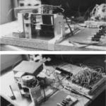
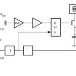
In 1987, your author built his first prototype of a laser scanner to be used as an automatic door opening and safety sensor. It was based on pulsed light emitted by a fast and powerful laser diode. The light scanned the scenery, deflected by a rotating mirror. Reflected light was received by a fast photo diode and amplified with an amplifier built with gigahertz bipolar transistors. Time was measured by an analog integrator, which was started with the firing of the laser diode and stopped with the reflected light pulse at the output of the amplifier. The result was a scanner that measured 10,000 distances per second with a 2-ns accuracy. Such an accuracy means a 30-cm accuracy in the system, which was quite impressive at the time.
However, intended applications were sensors that open automatic doors and safeguard the humans and goods between closing door wings of automatic doors. Such applications require a distance resolution in the 1-cm range. Due to the very high propagation speed of light in space, ultrafast photoelectronic devices and electronic circuits are needed. The lidar technology at that time had a timing resolution in the range of a few nanoseconds, which allowed the measuring of distances with a resolution in the range of 1 m. To achieve 1-cm resolution, the system had to be 100 times faster to allow time measurement with a resolution in the tens of picoseconds.
Basic Research for TOF
Designing a camera that can measure distances with a resolution and accuracy in the 1-cm range or tens of picoseconds in time resolution, simultaneously in tens of thousands of pixels and under full sunlight, is not something that can be achieved overnight. Even today, the challenges are huge, and few companies are able to manage these challenges. CEDES was one of the first companies worldwide that could manage the 1-cm resolution. But, CEDES failed to provide a system that works under full sunlight. To focus on only this goal, your author established a dedicated company, ESPROS Photonics Corp. The cornerstones of the technology development at ESPROS were:
- High near-infrared sensitivity (NIR)
- High-performance charge-coupled devices (CCD)
- Full mixed-signal complementary metal–oxide–semiconductor (CMOS) functionality
These key requirements seemed to be impossible to be combined on one monolithic silicon chip, because CCD and CMOS don’t “like” each other, and high NIR sensitivity is not possible with low-cost CMOS.
A pivotal requirement for the development was the maximization of the quantum efficiency over a broad wavelength range reaching well into the NIR. Today’s imaging applications are not confined to a specific wavelength. From classic consumer and performance imaging in the visible spectrum to infrared operation in industrial applications (and, further, to multispectral and hyper-spectral images in space), each application typically requires a specific range. Naturally, the more an imager process is able to cover, the higher the potential for success. Furthermore, as noise is always an issue in imaging, any increase in quantum efficiency will basically improve the noise behavior, with all other factors being equal. There’s simply more charge available to create a signal.
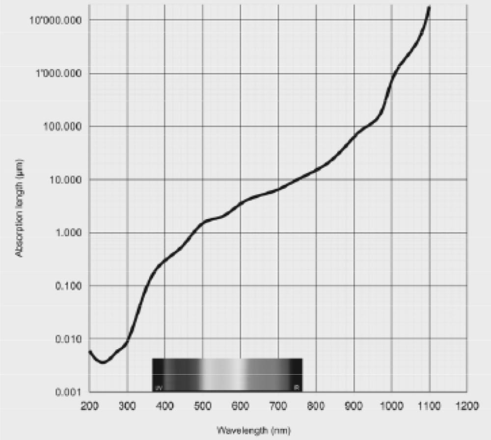
The absorption length of light in silicon inherently determines the quantum efficiency. It stands to reason that choosing the thickness of the depleted detector area is the favorable design parameter.
Figure 3 presents the most important parameter with regard to the quantum efficiency. It shows how deep light penetrates into silicon until it is fully absorbed. As can be seen, light in the visible domain between 400 and 750 nm penetrates some 100 nm to just a few micrometers into silicon. A thin active layer of silicon is good enough to achieve a good sensitivity. However, in the NIR domain (in the region of 800-1,100 nm), silicon becomes more and more transparent for light. Thus, a thick active layer in the tens of micrometers is needed.
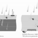
The choice of a suitable substrate material contributes, among other things, to a fully depleted detector thickness of 50 µm in CEDES epc imagers (Figure 4). This figure clearly shows why the sensitivity of the ESPROS technology is so much higher than what can be achieved with standard CMOS technology. However, to master that is not easy, and it took almost a decade from the idea’s inception to make it until it really worked. Figure 5 shows the long way to a first 3D TOF pixel: Christmas 2009 (left) to the first fully integrated 3D TOF camera on a chip in 2012 (middle) to the high-performance quarter video graphics array (QVGA) 3D TOF imager in 2015. The chip in the middle has a size of 2.5 X 2.5 mm2 and contains roughly half a million transistors. The QVGA imager on the right has a size of 8 X 9 mm2 and contains four million transistors.
30-Year Research
As previously explained, full basic research was necessary to achieve the required performance — ambient light suppression and high sensitivity were especially important.
Today, many different markets are mature for 3D TOF technology. When CEDES started its research 30 years ago, not many of us thought about drones or autonomous driving. Who thought about automatic vacuum cleaners or caretaking robots for the elderly or handicapped people at that time? Such applications are the drivers for cost-effective solutions because of mass production for mass markets. Imagers like this are very complex devices, the development costs for which are huge. But, once available, they are very cost effective and ideal to be integrated into devices in the Internet of Things (IoT) or Industry 4.0.
Deployment in the Elevator/Escalator Industry
The first use of a sensor using a 3D TOF camera is to replace today’s light curtains. Light curtains were commercialized 25 years ago, when they started to replace single-light barriers or mechanical safety edges.
Today, it is standard to safeguard the elevator door entry. However, light curtains are quite big parts – typically, two sticks, each with a length of 2 m, installed either dynamically at the door panels or statically at the car. They contain hundreds of components and all have the disadvantage of not really protecting the passengers, because they only monitor the area between the car door and the landing door. The leading edges of the elevator doors are not monitored, which can allow for serious accidents.
A sensor like that shown in Figure 7 protects the full door area with a size of only 10 X 2 X 2 cm3. Because of the very high degree of integration, many fewer components are needed, which leads to a much higher reliability.
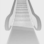
Another candidate for the application of a 3D TOF sensor is the escalator. Today, energy-savings operations of escalators need a control that slows or entirely stops the escalator motor if there is no demand for the escalator. However, when people approach the unit, it should restart immediately. False triggering of the sensors that signal to start the escalator is common today, e.g., if people pass by the front of an escalator with no intention of using it, the escalator starts its operation.
By using a 3D TOF sensor as shown in Figure 8, people flow toward the escalator only triggers the start of the motor. Crossing people flow has no effect due to the image-processing capabilities of the sensor. Another application of this sensor is to slow down or entirely stop the escalator if the people at the end of the unit do not move away. This can avoid a very dangerous situation that is often the root cause of accidents.
Conclusion
3D TOF imaging has matured enough to be deployed in many applications. Its readiness comes together with the demand for this technology because of the IoT and Industry 4.0 megatrend. High-volume applications like autonomous driving, drones, home appliances, etc. reduce the cost of this technology, which allows its deployment in elevator field applications.
Acknowledgements
During your author’s journey in the 3D-TOF field since 1985, several persons encouraged and supported him. Without their contribution, this work would not have been possible. Your author would like the express great gratitude to his wife, Brigitte, who always stands behind him, especially when it was very difficult to continue work within CEDES and ESPROS.
A major inspiration of your author’s work came from Peter Seitz, with whom he shared a very long part of his journey during the R&D of the lock-in pixel and its practical implementation. Important fundamental work was performed by many employees of ESPROS, but some particularly important contributors were Martin Popp, Bettina Weder, Marcel Rueegg, Dieter Kägi, Gion-Pol Catregn, Hanspeter Keller and Markus Ledergerber, among many others. Special thanks go to those who provided fundamental insight with their R&D of 3D-TOF systems.
- Figure 1: Your author’s first 3D TOF camera, built in 1987
- Figure 2: Block diagram of the laser scanner as a first functional TOF camera
- Figure 3: Absorption length of light in silicon; courtesy of ESPROS
- Figure 4: Standard CMOS versus ESPROS 3D TOF imager technology
- Figure 5: ESPROS’ 3D TOF history
- Figure 6: Light curtain sticks; courtesy of CEDES
- Figure 7: 3D TOF elevator door safety sensor (installed at the car door transom)
- Figure 8: 3D TOF sensor to start the operation of an escalator in energy-savings mode
- Table 1: History of CEDES’ and ESPROS’ 3D TOF development
References
[1] De Coi, B.; Popp, M.; and Marchesi, E. “White paper in imaging: CMOS vs. CCD” (2012).
[2] C. Hülsmeyer. German patent application no. 165546: “Verfahren, um Entfernte Metallische Gegenstände Mittels Elektrischer Wellen Einem Beobachter zu Melden” (1904).
[3] Wikipedia. “Radar Development” (2016).
Get more of Elevator World. Sign up for our free e-newsletter.
