Working with JFETs
Oct 1, 2015

Details on and how to deal with junction field-effect transistors (JFETs) on the job
JFETS are composed of N- and P-type crystalline silicon layers that have been doped. The underlying principles involving charge carriers – electrons and holes – are similar to those for diodes and bipolar transistors, as covered in previous articles (ELEVATOR WORLD, August and December 2014). Though simpler to understand, the JFET proved more difficult to build (at first) than the bipolar transistor.
Learning Objectives
After reading this article, you should have learned:
♦ What makes up JFETs and their basic characteristics
♦ How a JFET works
♦ The differences and benefits of N- and P-channel JFETs
♦ JFETs’ role in the digital revolution
♦ How to troubleshoot and test digital circuitry containing JFETs
Purpose
The JFET has always had palpable advantages over the bipolar transistor, and, for a while, it dominated the three-wire semiconductor scene until it, in turn, was pushed aside by the metal-oxide semiconductor field-effect transistor (MOSFET), which eventually triumphed both as a discrete component and within integrated circuits (ICs) (EW, October 2014). Because the MOSFET’s gate is insulated from the channel, input impedance is even higher than that of the JFET. The current drawn from the preceding stage is very low, so the output circuit is loaded only an infinitesimal amount. For this reason and others, MOSFETs are manufactured in great numbers, both as discrete components and within ICs. Still, there are many JFETs around in older equipment that now requires maintenance and servicing, and JFETs are the components of choice in special applications.
We previously saw that diodes are formed when N- and P-type crystalline silicon with leads attached join to form two layers with a junction between them (EW, August 2014). In contrast, bipolar transistors are made up of three layers, (negative-positive-negative or positive-negative-positive), each having a lead and two junctions separating them (EW, December 2014).
Current flow in the input circuit regulates much heavier current flow in the output circuit. That accounts for amplification, oscillation and other useful phenomena. The JFET makes use of the same semiconductor properties, but the structure and electrical parameters differ. This can make for difficulties in testing and diagnosis without a full understanding of what is going on with the electrons and holes.
Composition
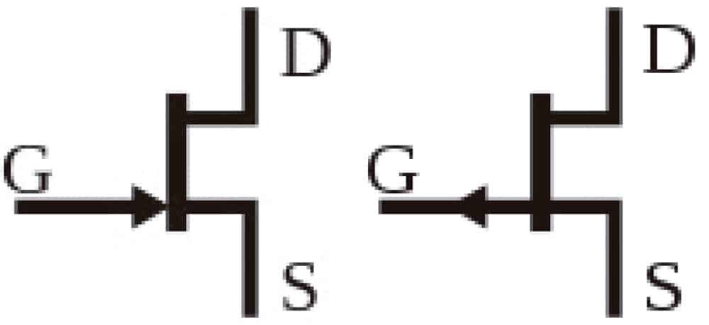
Rather than a small cylinder with three leads emerging from one end, the JFET more often resembles a flat disc. In a bipolar transistor, the current flow from base to emitter controls the much larger current flow from emitter to collector. Rather than base, emitter and collector, in the JFET, there is a gate, source and drain. (Actually, there are two gates, one on either side of the device. They are usually wired together internally, so, in essence, they are a single element.) Source and drain are at either end of a doped semiconductor known as the channel. It may be N- or P-type.
The source and drain comprise the output circuit. As in any transistor, the output section is basically a resistor. The resistance varies, often at very high speed, in accordance with the signal applied to the input terminals. This signal, in a bipolar transistor, causes variations in the amount of current flowing between the base and emitter. It is here that the situation for a JFET is different. Rather than current flow in the input circuit, the operative event is an electrical charge imposed upon the gate.
Of course, this voltage has to be referenced to something, and that is the source. The gate and the source, taken together, make up a diode, since they are opposite types (N and P) of semiconducting crystalline silicon. When reverse biased, there is very high impedance between them. You can imagine the minute amount of current required to impose an electrical charge on such small bodies as the two gates. Therefore, a defining characteristic of the JFET is that it has extremely high input impedance, on the order of 100 megohms. It does not tend to load the upstream circuit, which, in many instances, is highly favorable. In fact, an important application for the JFET has been as a front-end amplification stage in a digital voltmeter, where it is desirable to be invisible to the circuit under test, especially if that circuit is high impedance and vulnerable to loading. Of course, all of this depends upon the JFET’s input circuit being reverse biased; so, if the polarity is wrong and the device is forward biased, the transistor is destroyed.
Structure
JFETs are available in N- and P-channel versions. In the N-channel device, there is a surplus of electrons in the channel, and they function as charge carriers. The source and drain are also made of N-channel crystalline silicon. They are attached at either end. The gate is the opposite type. When it has a potential with respect to the source of 0 V, current through the channel is at the maximum. Then, as negative voltage increases, the electrons are repelled away from the gate so that the channel, in effect, becomes narrower and less conductive. Current through the output circuit varies with voltage on the input terminal. The channel is built upon a crystalline silicon substrate that has been doped to make it the opposite type. This substrate may or may not be electrically connected to the supporting circuitry. It is primarily useful when the JFET is part of an integrated circuit.
In a P-channel JFET, the charge carriers are holes, rather than electrons. Here again, maximum current in the channel occurs when the gate is at 0 V potential with respect to the source. As the gate becomes more highly charged in a positive direction, the holes are repelled until the channel becomes effectively closed, at which point the current drops to 0. At this point, the device is saturated, and further increase in voltage on the gate has no direct effect on channel conduction. The voltage level on the gate that reduces current flow in the device to 0 is known as the “pinch-off voltage.” That and other electrical and physical parameters are given in the manufacturer’s datasheet.
In accordance with Kirchhoff’s Current Law, the amount of current is the same throughout source, channel and drain, both internally and in the exterior circuit. Since there is only one semiconductor type in this output circuit, it is symmetrical, and, in theory, source and drain terminals are interchangeable. In actual practice, however, when the drain power supply exceeds 0.6 V, distortion in the shape of the channel’s conductive zone occurs, decreasing its size as it approaches the drain. For this reason, in an N-channel JFET, the positive voltage should be applied to the drain only.
Configuration
As an amplifier, the JFET may be used in any of these configurations: common gate, common source and common drain. The common gate amplifier corresponds to the bipolar transistor’s common-base setup. Despite being the most fundamental application, it is actually seen less frequently than the other configurations. It is, however, the circuit of choice when the amplifier is required to operate at or near the JFET’s upper frequency limit. The common gate configuration provides high voltage gain but low current gain; overall, the power gain is less than that in other configurations. Unlike many amplifiers, the input and output are in phase for both N- and P-type channel devices. Input impedance is low, while output impedance is high.
The most widely used JFET amplifier configuration is the common-source hookup. The bipolar transistor equivalent is the common-emitter circuit. Power gain is high, and input impedance is much higher than in the bipolar circuits, though lower than that exhibited by MOSFETs. Input and output waveforms are 180 degrees out of phase, which is not at all a drawback as long as it is taken into consideration. If there are two or any other even number of stages, the ultimate output is brought back into phase with the input at the first stage.
The common-drain amplifier configuration is also known as the “source-follower.” It provides excellent buffering and high input impedance, meaning that there is minimal loading of the preceding stage. In both N- and P-channel JFETs, input and output are in phase.
Digital Application
So far, this article has examined JFETs as used as analog devices only. But, the truth is that JFETs (along with other semiconductor devices) have played an essential role in the digital revolution that has remade electronics and our newly networked world.
The underlying concept in digital technology is that rather than power – electrical and mechanical – it is information that is processed. Then, thought becomes action: Elevators (to take one example) travel the vertical length of our high-rise buildings, opening and closing doors for passengers, responding to the fire alarm system and statistical traffic patterns as though they were capable of conscious thought.
The basis of the digital domain is binary. Only two integers are employed (0 and 1) corresponding to different voltage levels within and outside the crystalline silicon semiconductors. Zero is “off” (electrically) and false (logically), and 1 is “on” and “true.”
Logic gates can be built using electromechanical relays, hydraulics, pneumatics, molecules, optical devices or various combinations of cogs and gears. In electronic equipment, our interest is mostly in silicon semiconducting devices – diodes and transistors – because of their extraordinary reliability, high-speed operation, low power consumption, small size, availability in many variations and low cost.
There are seven basic digital logic gates. (Inputs are always shown on the left, and outputs are on the right.) They are:
- AND: there are two (or more) inputs and one output. If both inputs are 1, the output is 1. If one (or more) input is 0, the output is 0.
- OR: if one or both inputs are 1, the output is 1. If all inputs are 0, the output is 0.
- XOR (EXCLUSIVE-OR): this gate produces a 1 output if either (but not both) output is 1.
- NOT: a logic inverter, this gate produces a 0 output if the input is 1 and a 1 output if the input is 0.
- NAND: this produces 0 output if both inputs are 1. If one or both inputs are 0, it produces a 1 output.
- NOR: the output is 1 if both inputs are 0. Otherwise, the output will be 0.
- XNOR: the output is 1 if both inputs are the same and 0 if the two outputs are different.
Logic gates are the building blocks of digital circuits, and in this area, the MOSFET has become dominant, pushing the JFET aside to a certain extent. But, simultaneously, the scenario has come to include another device, the metal semiconductor field-effect transistor (MESFET). In a supporting role is the Schottky barrier diode (SBD), which joins the MESFET to form a single device built on the same substrate but separated by an isolation region that is not electrically active.
The devices covered so far have been silicon based, but for digital applications requiring high speeds, it was necessary to look elsewhere. While it is true that electrons travel at a major fraction of the speed of light depending on the medium, much greater periods of time are required for them to get into and out of semiconducting devices. And, where there are sometimes millions of diodes and transistors in an IC, this latency can be a problem. That is why certain programs on computers (especially graphic applications such as Aperture) may be slow acting even when the computer is not connected to a network and the hard drive is not running.
To remedy this situation, engineers have turned toward gallium arsenide (GaAs), which is a compound formed of gallium and arsenic. Electrons travel much faster in N-type GaAs than in silicon. Semiconducting devices so made, for the same input voltages, have much higher output current, translating into greater gain. With higher output current, charging and discharging of load and parasitic capacitances occur at a higher rate, the outcome being increased operating speed.
GaAs devices have found a secure niche in high-speed ICs for digital equipment operating far in excess of 100 mHz. An example of this technology is the MESFET containing the SBD noted above. The common GaAs substrate is not doped and, therefore, is not very conductive. Advantages in this construction are that the devices are insulated from one another when integrated into a microchip. Moreover, parasitic capacitances between the device and circuit ground are reduced.
The MESFET gate is directly connected to the Schottky-barrier diode’s anode. The anode and cathode are bonded to heavily doped Type-N material, as are the source and drain in the MESFET section. The gate is bonded to a more lightly doped piece of Type-N GaAs, which forms the channel. To facilitate high-speed operation, the channel is made as short as possible.
Operation of the MESFET is similar to a silicon JFET, but the electrical parameters are different. These devices are available in N-channel versions only because the behavior of holes in a P-channel MESFET have proved problematic due to relatively sluggish drift mobility within the channel.
Digital circuitry also containing JFETs as discrete components within ICs is subject to failure because of the vast number of connected pieces. When failure happens, the electronic technician is called upon to restore functionality.
Troubleshooting
The troubleshooting and repair process may range from the incredibly simple (such as resetting a branch-circuit overcurrent device) to something so difficult that the technician is pushed to the very limit of his or her knowledge and expertise, in which case it is best to regard it as a valuable learning experience and maintain a positive attitude. Don’t expect to fix everything within a few minutes. Sometimes, it requires patience and methodical information gathering before real progress occurs.
When it comes to digital troubleshooting, you need the right tools, and these fall into two categories: knowledge (including product-specific documentation) and good test equipment. As for documentation, a large amount is available on the Internet.
As an example, let us say that an elevator has quit running. The alphanumeric readout may give a cryptic error code. If the operating manual is available, you should be able to look up the error code and discover the problem, along with a suggested remedy. If the operating manual is not available, it can likely be downloaded from the manufacturer’s website. On the Internet, in addition to acquiring product-specific documentation from the manufacturer, typing the make, model and specific concern into a search engine can provide numerous technical forums and tutorials covering equipment-specific problems. When physical difficulties arise, such as getting a cabinet apart in a nondestructive fashion so as to access the chassis, YouTube videos are a great help.
The best time to make preparations is before trouble erupts. Adjacent to critical control panels and motors, install a phone jack and post the number of the manufacturer’s technical help line, along with make and model numbers that may be difficult to find quickly on the nameplate. Additionally, copies of operating and installation manuals and schematics should be housed in a clearly marked cabinet nearby.
Any equipment essential to safety or for continuous operations – an elevator in a public place comes to mind – should be the subject of thorough preparation prior to any malfunction. Thermal imaging and an ongoing program of torqueing high-current terminations should be part of the picture.
Before looking at the low-power semiconductors, verify the main power flow. Typically, in large equipment, there is a three-phase main feed with a disconnect (capable of being locked out) that goes to the controller cabinet. Here, if the voltage is not too high, power on all three legs can be checked with a voltmeter. Thence to a rectifier. When the equipment won’t run, diodes and large electrolytic capacitors are frequent culprits. Check visually for any sign of distortion or burning before making meter checks.
If there is a DC bus as in a variable-frequency drive, it is advised to look at both ends with an oscilloscope. The DC voltage should look clean and uniform with minimal ripple or harmonics. The best way to get a sense of this for the specific equipment is to take readings at a time when the equipment is functioning normally. For critical machinery, it is important to take readings at regular intervals to spot harmful trends before there is an outage. Post a log next to the equipment so results can be posted for periodic comparisons.
If everything looks good in terms of main power paths, it is time to look at the control circuitry, which will consist of one (or more) circuit board. Since the voltage and current levels are much lower, faulty components will not likely be able to be detected visually (by a burnt or distorted appearance). Also, troubleshooting and diagnosis are more difficult due to circuit complexity. Printed circuit boards are becoming more densely populated with ever smaller and more numerous components, which means the current paths are more difficult to trace. Consequently, the trend has become to replace entire circuit boards, as opposed to individual components. The difficulty here is that the boards (or “cards,” as the smaller ones are known) have become quite expensive. If one purchases and replaces a US$400 board and the equipment still does not work, his or her knowledge and judgment will be questioned. Due to low cost, it is feasible to keep an inventory of components and replace them as needed. On a tight board, it is necessary to employ impeccable soldering, heatsinking and static-protection techniques.
The tools of the trade, besides documentation including schematics, are multimeter, oscilloscope and logic probe. The logic probe is generally circuit powered, and it differentiates the unique high and low states for the principle logic types. Complete instructions for use, available models and plans for building them may be found on the Internet.
Transistor testing, including JFETs, is best accomplished with a specialized meter: just connect the leads and read the results. Alternatively, a multimeter (with or without the diode test function) may be used. Refer to the previously mentioned EW articles on transistors for the complete procedure using nothing more than the ohmmeter function.
Learning-Reinforcement Questions
Use the below learning-reinforcement questions to study for the Continuing Education Assessment Exam available online at www.elevatorbooks.com or on p. 173 of this issue.
♦ In a JFET, which terminals correspond to base, emitter and collector?
♦ Which terminals comprise the output circuit in a JFET?
♦ What is the typical input impedance in a JFET?
♦ What happens if the input circuit in a JFET becomes forward biased?
♦ Why did the MOSFET replace the JFET in most applications?
Get more of Elevator World. Sign up for our free e-newsletter.


