Integrated Circuits
Mar 1, 2015
The history, application and maintenance of these important microelectronics components are explored.
In the microelectronics continuum, integrated circuits (ICs) are probably close to their midpoint of development. They have progressed far since their inception around the middle of the last century, but for the “smaller is better” theory, there is no endpoint in sight. To begin this survey, we will peer back into the past to see how IC technology emerged from a more primitive semiconductor environment. Naturally, the most primitive of these precursor devices were diodes (ELEVATOR WORLD, August 2014), because only a single junction was involved.
Learning Objectives
After reading this article, you should have learned about:
♦ The emergence of IC technology
♦ How Moore’s Law affects IC development
♦ Limits to IC development
♦ The importance of differential amplifiers in IC applications
♦ How to troubleshoot and repair ICs in elevator controllers
The device performed better than the old-world diode vacuum tube, and as increasingly refined production methods emerged, the cost to the end user fell sharply. Simultaneously, a two-junction device with three leads appeared. The transistor made tubeless radios possible, and TVs became far more compact and energy efficient. This was the underlying situation when IC technology, very limited and tentative in form by today’s standards, first appeared.
In 1949, a Siemens engineer, Werner Jacobi, filed a patent for an important IC precursor: a three-stage amplifier, the five transistors occupying a common substrate. The goal was to miniaturize the previously clunky hearing aid. The DC device, as conceived at that time, did not go into production, but the underlying idea became part of the intellectual underpinning that made further developments possible.
In 1952, Geoffrey Dummer, a radar scientist at the British Ministry of Defense Royal Radar Establishment, wrote a paper that laid out the basic idea of the IC, but he was unable to actually build the device. In mid 1958, a major breakthrough was achieved by Jack Kirby, working for Texas Instruments. He proposed the IC as we know it, and later that year, he built the first working model of it. Kirby’s device was built on a germanium substrate. Less than a year later, Robert Royce designed a chip with a silicon substrate. It was produced by Fairchild Semiconductor and represented a substantial step forward.
IC development in the years that followed was characterized by the capability to place an ever-increasing number of transistors on a single chip. “Small-scale integration” is the term given for the first stage in this progression. It refers to the technology that prevailed in the early years, when the number of transistors that could be integrated on a single substrate was fewer than 100. These chips constituted the electronic brains for the Minuteman Missile and Apollo programs, in which weight was at a premium.
Successive chip densities were “medium-scale integration,” “large-scale integration,” “very-large-scale integration” and “ultra-large-scale integration.” The boundaries between these levels are not meaningful in any definitive sense, except to suggest what can only be described as an explosion in our capability to create huge numbers of digital logic gates in increasingly smaller packages. This progress is described by Moore’s Law, which states that the number of transistors we can place in a single chip doubles every two years, or, in another version, every 18 months. While an accurate description of the current state of integration, this statement (which is more an observation than an actual law) is somewhat fanciful, because it suggests that before long, there will be more devices in the densest microchips than there are elementary particles in our universe.
Notwithstanding, the level of integration that has been achieved is astounding. Currently, single ICs are being manufactured that contain devices numbering in the tens of billions. This fact has been made possible by the development of complementary metal oxide semiconductor (CMOS) technology. This technology refers not to a single device, but to a circuit composed, in its most basic form, of two metal-oxide semiconductor field-effect transistors (MOSFETs), a P-type and an N-type, connected in series with respect to the applied bias (EW, October 2014). Since one of them is off while the other is on, there is no current flow, except very briefly during transitions. Consequently, there is minimal heat generation, even in the dense configurations in VLSI and beyond. Without CMOS, there would be no International Space Station as we know it.
There are other “brick walls” that may neutralize Moore’s Law, perhaps hindering our ability to migrate beyond this temporally finite solar system. For one thing, miniaturization can only go so far before theoretical, practical and economic limits are approached. The latest thinking seems to be that Moore’s Law will evolve. It is becoming apparent that circuits the size of single molecules are feasible thanks to the use of nanomaterials. These are metals, ceramics and polymeric materials that resemble living organisms, because they have the capability of designing and replicating themselves.
The value of this miniaturization goes far beyond just the idea of creating increasingly compact consumer devices, although that is one benefit. Smaller chips with greater circuit density means the connecting media traces required for internal wiring become shorter and thinner, vastly increasing the speed of the device and reducing cost. A theorized material called stanene, composed of a one-atom-thick sheet of tin, could act much like a room-temperature superconductor.[1] This and other innovations stand to pave the way for higher-performance ICs.
Like most other semiconductors, ICs are constructed using planar processes on microcrystalline silicon wafers. The essential stages are thin film, lithography, etching and doping. To begin, SiO2 and polycrystalline films are bonded to the silicon substrate. The next layer is a photo-resistive or light-sensitive layer exposed to light through a mask. The product is next placed into a developer, causing the areas that had been exposed to light to dissolve. This leaves the areas that had not been exposed to light intact.
Lithography consists of duplicating the mask pattern at the photoresist level, which becomes the mask for the etching process. The photoresist layer is then eliminated by the application of suitable chemicals, readying the semiconductor material for doping. In this process, very slight amounts of specific impurities are added. At the P-N junctions, charge carriers, electrons and holes, are available so that conduction can take place when needed and not take place when not needed, in response to the amount and polarity of the applied bias.
Doping is a subtle undertaking. Typically, a gas is passed over the substrate for a period of less than 12 hours. Depending upon the desired electronic properties, doping will be light or heavy. For light doping, the concentration is on the order of one atom of the impurity per 100 million atoms of the P- or N-type material, while for heavy doping, the ratio is 1:10,000. These very slight concentrations convert uninteresting slabs of fused beach sand into the building blocks for intelligent machines.
The workflow described above is repeated as needed to build the IC on its substrate. More than 600 steps may be required to manufacture a typical IC. At any stage, an errant speck of dust or inaccurate temperature, timing or alignment can invalidate the entire process. Therefore, extensive testing is needed at each step. Testing can account for up to 25% of production costs.
Because billions of transistors may inhabit a single chip, it is obvious that no single individual (nor even a working committee) could understand the architecture in all its complexity. For this reason, the design phase of these miraculous entities has become largely automated.
IC design theory differs, depending upon whether the chip is digital or analog. Examples of digital components are random-access memory, read-only memory, flash computer memories, field-programmable gate arrays and all sorts of application-specific integrated circuits. Examples of analog ICs are operational amplifiers (opamps), lineal regulators, phase-locked loops, oscillators and active filters. Since signal fidelity in analog ICs is the focus (in contrast to the up or down digitals), analog devices are usually larger with less circuit density. Accordingly, the design goals and procedures differ sharply.
Electronic design automation (EDA) refers to numerous software tools that work for both printed circuit boards (PCBs) and ICs. The goal is to thoroughly simulate and test ICs prior to manufacture. As semiconductor technology has evolved to a point where immense numbers of devices are packed into ever-smaller ICs, EDA has become the only viable means for meeting the design goals, which are numerous. After circuitry has been designed, simulated, tested and verified, engineers move on to the physical design. Here, again, complexities abound.
Gross structural arrangement is first on the agenda. Register-transfer level (RTL) analysis applies to the flow of signals between registers, which are assigned to locations inside the IC. Cores and arrays are assigned, and input/output pins are determined. Then, a netlist (a list of all the component terminals that should be electrically connected for the circuit to work) of required gates is generated. Clocks are added for timing the workflow, and wiring is connected. (All of this is on a conceptual level, and the plan is to create a finished design that works prior to physical implementation.) Following satisfactory completion and verification, it is necessary to step back and ascertain whether the chip, so conceived, can actually be manufactured. Electrical, physical and economic goals must be considered before the IC can go into production.
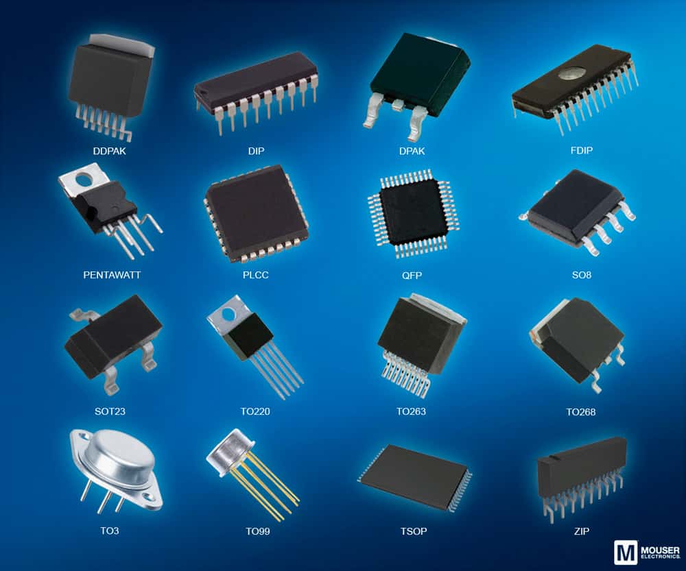
Choice of packaging is critical during the design process so that the chip will function properly within the contexts of various types of electronic equipment contemplated. A good knowledge of IC packaging is also important for technicians who intend to troubleshoot and repair the machines.
IC packages have been ceramic or metal in the past, but now, plastic prevails. Each type of package is designated by a letter or letter/number combination. The packages are various sizes and shapes with different numbers and configurations of pins. Inside the package is the chip proper, known as the die, with terminations far too small to be hand soldered. (Also, the heat would instantly fry the sensitive chip.) Attached to the die are gold-plated leads that are, in turn, connected to the conductive pins outside the package. These can be soldered, but care must be taken to prevent heat or static electricity from traveling into the semiconductor material. Unless overcome by curiosity, technicians will not have occasion to break open these packages, since the chip is not repairable.
The pins serve two purposes: to physically mount the chip and to connect it electrically to the outside world. Of course, the pins have to be installed correctly. Many semiconductors are incinerated if the power-supply polarity is inadvertently reversed, although a blocking diode or protective fusing can sometimes prevent damage.
ICs usually have a dot and/or notch at some point along their perimeter. This marks the spot where pin numbering begins, starting with one and proceeding in a counterclockwise direction looking down at the top of the IC. The pin connections are identified by number in the manufacturer’s datasheet, available as a free download on the Internet. Additionally, there are archival sites, on which datasheets for obsolete or out-of-production ICs can be found.
These chips are available in two categories, based on how they mount on the circuit board. Through-hole packages are larger and more user friendly if the device needs to be replaced or taken out of circuit for testing purposes: simply insert the pins through the holes in the board, flip it over and solder on the back side, then snip off the excess. Surface-mounted packages are very small and more difficult to replace or remove for testing. They are positioned on one side of the board and soldered in place. Special tools and techniques are required.
Although the very basic 555 IC is known as a “timer,” it is capable of performing other functions, as well. Besides providing time delays of various durations and intervals (together comprising the duty cycle), the 555 can work as an oscillator, flip-flop device, make a push-button switch bounce free and function as a sensor, among numerous other applications, by means of external circuitry.
Most equipment with a blinking LED, such as many telephones and printers, utilize 555 ICs. These circuits, along with accompanying LEDs and resistor-capacitor (RC) networks, can be harvested from retired units, but with 555s priced at less than US$1, this is hardly worth the effort.
Signetics (later acquired by Philips) introduced the 555 in 1971. It is now made by numerous manufacturers with some internal variation and slightly differing operating characteristics and part numbers but identical pinouts. With small variations, the 555 contains a mere 25 transistors, 15 resistors and two diodes. It is available in an eight-pin dual in-line package. There are other versions, such as the 556, which consists of a single chip containing two 555s in a 14-pin dual in-line package. Other variations are the 558 and 559, consisting of 16-pin dual in-line packages containing four 555s. CMOS technology is invoked to create the low-power TLC 555.
The standard eight-pin 555 in a dual in-line package illustrates the simplicity and multiple functions of this remarkable device. As always, pins are numbered consecutively from the dot/notch, beginning with pin 1 and proceeding counter-clockwise:
- Pin 1, GROUND: Provides the low-level reference
- Pin 2, TRIGGER: A timing interval begins, and pin 3, OUT, goes high when this input drops below half of the voltage applied to pin 5, CONTROL.
- Pin 3, OUT: This output goes 1.7 V below Pin 1, GROUND, when triggered.
- Pin 4, RESET: The timing interval resets when this input is connected to pin 1, GROUND.
- Pin 5, CONTROL: Varies the timing of the RC network
- Pin 6, THRESHOLD: Detects two-thirds of rail voltage, making OUTPUT low if pin 6, TRIGGER, is high.
- Pin 7, DISCHARGE: Becomes low when Pin 6, THRESHOLD, sees two-thirds of rail voltage.
- Pin 8, SUPPLY: Must be connected to the positive supply voltage for the IC to work: acceptable range is 4.5-15 VDC. For digital applications, use +5 VDC.
The 555 has three operating modes: monostable, astable (free running) and bistable (Schmitt trigger). In the monostable mode, the 555 is a one-shot pulse generator. When the trigger pin sees a voltage less than one-third the supply voltage, the pulse begins. The duration depends upon the values of the resistor and capacitor in the RC network. After this single pulse, the IC remains dormant until it is retriggered.
In the astable mode, the 555 becomes an oscillator. At slow speeds, it can cause an LED to flash, or it can function as a logic clock. It can also be used to create audible tones.
In the bistable mode, the 555 becomes a flip-flop. Pin 7, DISCHARGE, is not connected, and the external capacitor is not present. An important application is the bounce-free switch, made possible by the latching action of the 555, operating in its bistable mode.
Due to its simplicity, tolerance of a wide range of supply voltages, multiplicity of applications and low cost, the 555 is a good introduction to the world of ICs. With a low pin count, equipment in which it is used is easy to troubleshoot and repair. Somewhat more expertise is required in dealing with the opamp, but because of its frequent occurrence, it should be part of technicians’ knowledge base.
Early analog computers containing opamps consisted of huge arrays of vacuum tubes with high-voltage power supplies. There was lots of heat to be dissipated, and the dedicated space for doing this was substantial, so the machines were mostly seen in universities and large research facilities. Today, with solid-state electronics and the ubiquitous IC, opamps are common enough to be found in almost every home. They also figure prominently in heavy commercial and industrial equipment. Because of their wide usage, they are worth a close look.
The opamp is one (but not the only) type of differential amplifier. It resembles the fully differential amplifier, which differs by having two outputs. The opamp has one output and two inputs. The inputs are V+ and V-, so one is the inverse of the other. The IC, due to internal circuitry, amplifies only the difference in voltage between the two. The degree of amplification conforms to this formula:
VOUT = AOL (V+ – V–)
where VOUT is output voltage, V+ is non-inverting input, V– is inverting input, and AOL is open-loop gain.
The open-loop gain is relevant in cases where there is no feedback connection between output and input. Because of the enormous gain of an opamp in the open-loop mode (often around 100,000), the degree of amplification is phenomenal. But, the real advantage of this IC is seen when it is operated in the closed-loop mode. Here, the amplification is much less, given by this equation:
VOUT = VIN (1 + Rf/Rg)
where Rf and Rg are the values shown in Figure 4.
The opamp in this circuit is far more stable than either the open-loop opamp or previous amplifiers without negative feedback. The opamp, so configured, was designed to solve stability and noise problems that existed in the early years of radio and wire transmission. This is why long-distance callers don’t have to yell to hear each other.
Troubleshooting and repairing large-scale commercial and industrial electronic equipment, such as elevator controllers, usually involves analyzing the symptoms and (with the help of the manufacturer’s documentation and schematics) isolating the defective section, circuit and component. Not infrequently, the culprit is a bad IC. Sometimes, it will have a burnt or distorted appearance, or it will be abnormally hot. More likely, there will be no indication by outward appearance.
If cost is not a factor and the focus is getting the equipment up and running quickly, the repair may consist of replacing an entire circuit board. The problem with this solution is that individual boards can be very expensive, and a complete backup inventory would be quite large.
To a certain extent, it is possible to test an IC using a multimeter, especially if it has the “diode test” function. This procedure is helpful but not definitive. In it, the technician would consult the manufacturer’s datasheet and see where continuity should and should not be expected. If all pins are shorted out to the substrate, the IC is bad. There should never be a short between power and ground. Frequently, the manufacturer’s datasheet contains a schematic of a test circuit that can be built to test the IC on a go, no-go basis. A good plan would be to replace the defective circuit board, then take it back to the shop and replace the defective IC so a spare board is on hand for future use.
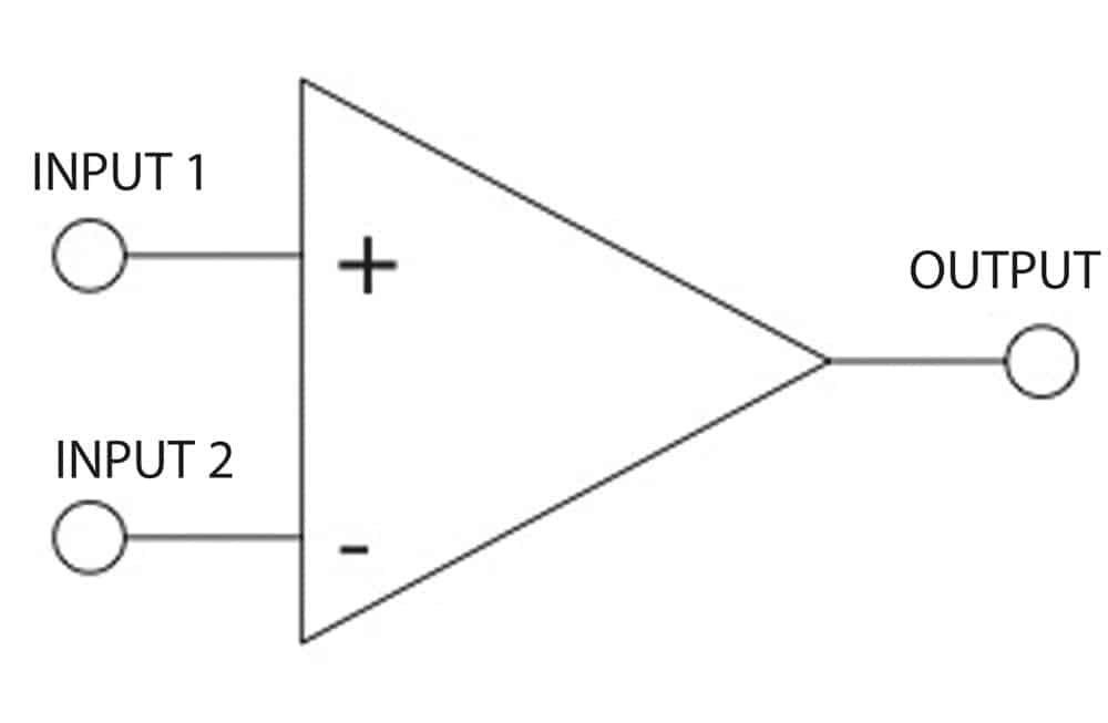
Figure 2: The opamp has two inputs of opposite polarity. The output is based upon the difference of the inputs. 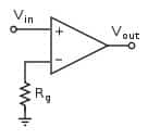
Figure 3: The open-loop opamp, with no feedback, has enormous amplification (graphic courtesy of Wikipedia). 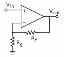
Figure 4: The closed-loop opamp is created by adding a feedback line from the output to the inverting input. Rf and Rg limit the amount of amplification, greatly improving stability and reducing noise. If more amplification is desired, additional stages can be cascaded (graphic courtesy of Wikipedia).
Learning-Reinforcement Questions
Use the below learning-reinforcement questions to study for the Continuing Education Assessment Exam available online at www.elevatorbooks.com or on p. 149 of this issue.
♦ Who built the first working IC?
♦ What is small-scale integration?
♦ What does Moore’s Law state?
♦ What does “CMOS” mean?
♦ How is lithography used in manufacturing ICs?
References
[1] Charles Q. Choi. “Could Atomically Thin Tin Transform Electronics?” Scientific American, December 4, 2013 (www.scientificamerican.com/article/could-atomically-thin-tin-transform-electronics).
Get more of Elevator World. Sign up for our free e-newsletter.


