MOSFETs
Oct 1, 2014

This article on metal-oxide semiconductor field-effect transistors (MOSFETs) builds on lessons from the prior piece “What Is a Diode?” (ELEVATOR WORLD, August 2014).
Metal-oxide semiconductor field-effect transistors (MOSFETs) are similar to the junction field-effect transistors (JFETs) that came before. In a MOSFET, the gate is insulated from the rest of the device by a layer of silicon dioxide. (Originally, the insulating material was a metal oxide. Despite the change, the old name persists.) If you understand how the insulated gate works structurally and electrically and all the implications that follow, you will comprehend the MOSFET to the extent that servicing electronic equipment that contains the device will be straightforward.
Learning Objectives
After reading this article, you should have learned about:
♦ Similarities and differences between MOSFETs and JFETs
♦ How to safely handle MOSFETs
♦ The importance of the two modes in which MOSFETs can operate
♦ How to switch current-carrying devices in elevator motors to make them perform as desired
♦ When MOSFETs are used in elevator motors and how to prevent premature insulation failure in motor windings
Basic Attributes
Because of the electrical barrier between the gate and the n- or p-type channel (NMOS or PMOS), the MOSFET has DC input impedance even higher than that of the JFET: in the nearly inconceivable vicinity of 10-100 million megohms. Compare this to the typical 200-meg temperature-corrected reading typical of the insulation surrounding a high-voltage transmission line. Additionally, this impedance is a property of a dielectric layer that may have a thickness of only a very few atoms. Since capacitance is a function of the dielectric constant of the insulating material and is inversely proportional to its thickness, we can calculate the capacitance of the gate-channel implicit capacitor as in the neighborhood of 2 fF, depending upon the electrical environment.
As in a JFET, the current flowing through the MOSFET channel is regulated not by current flowing through the input circuit, as in a bipolar transistor, but rather by voltage placed on the gate with reference to the source. The amount of current required to place a charge on such a small electrode can only be described as miniscule, so the MOSFET places virtually no load on the output circuit of the upstream device — that is to say, much less than the JFET. Another way to say this is that the MOSFET has extremely high input impedance, and this accounts for its value in many applications. To the device that feeds it, the MOSFET is invisible. At the same time, the MOSFET has a low output impedance so that it, in turn, is a stiff source that has little tendency to be loaded by the stage that follows it. The only downside of this is that caution is required when handling MOSFETs precisely because of the immense input impedance with its very thin dielectric barrier between gate and source/drain. The human body, brushing against a glass or plastic object, if not grounded, tends to acquire and retain an electrostatic charge that is very high in the context of the MOSFET (with its diaphanous internal structure).
Protecting MOSFETs
The bottom line is that without special precautions when removing a replacement MOSFET from its packaging and preparing to solder it in place, there is a high probability a technician will convert the device to a useless fragment of silicon so that, when the piece of equipment is put back in service, it will be found to work no better than before the repair. However, the MOSFET will exhibit no visible sign of such damage. To prevent this unfortunate occurrence, some precautions are in order. Manufacturers ordinarily ship MOSFETs packaged with the terminals pushed into conductive foam or shorted out with a copper wire to prevent the buildup of an electrostatic charge. If this is the case, keep the device shunted until immediately before installation. When handling the MOSFET, avoid touching the terminals. Do not allow the device to come into contact with plastic or fabric. Also, periodically touch a well-grounded conductive surface to drain out any potential you may have accumulated.
To prevent electrostatic charge, a commercially available grounding bracelet may be connected at the worksite and worn if MOSFETs are to be handled. You can make your own. Fashion a loose-fitting copper bracelet of 8 AWG bare solid copper wire and solder to it an appropriate length of 16 AWG insulated stranded wire for the ground connection. At the far end connect a phone jack of the type used for audio equipment. Install the female socket on a grounded enclosure. Be certain that the chassis is not the old-style floating-ground type that may become hot. You need an equipment ground bonded directly back to the equipment ground at the service. Ensure that there is no chance for your grounding bracelet to become isolated from ground, in which event you could lose the MOSFET, and no chance that it could become hot, in which event you could lose yourself. Do not wear the grounding bracelet when working on power equipment or on any circuit where you could contact a hazardous voltage.
The other source of a damaging electrostatic charge or stray current can be any sort of power tool, including a soldering iron, drill or electric solder sucker. The tip of a soldering iron should be grounded at all times. Even blowing compressed air across a printed circuit board can generate an electrostatic charge, so the technician should always be mindful of nearby MOSFETs when performing such tasks.
Electrostatic damage to a MOSFET can be insidious in that the damage may not show up immediately, but may be latent, causing premature component failure days, weeks or months down the road. One preventive measure is to humidify the air: for example, by keeping a pot of water boiling on a hotplate near the work area. Humid air continuously bleeds the electrostatic potential off a charged body so that it does not reach a damaging level.
To design or become proficient in the troubleshooting and repair of CMOS circuits, one must be aware of their steady-state and dynamic electrical behaviors.
Operation
In contrast to the MOSFET, the JFET operates in only one mode. When voltage on the gate (with reference to the source) is 0, the channel is as conductive as it is going to get. Then (for an n-type-channel device), if a negative voltage is applied, the channel narrows, becoming less conductive. At a certain level (to be found in the data sheet) known as “pinch-off,” the channel closes, and the device will no longer conduct. Because an application of voltage above the threshold level causes the current to diminish, then cease altogether, it is sometimes said that the JFET is operating in the depletion mode, but this terminology can be misleading, because there is no other mode for this device. The JFET should be reverse biased only. If it is forward biased, the current is limited only by maxing out the power supply, so the JFET will be destroyed.
The MOSFET, on the other hand, may operate in either a depletion or enhancement mode. In the enhancement mode, when 0 V is on the gate with reference to the source, the MOSFET does not conduct. If the applied voltage exceeds the threshold level, the device begins to conduct, and the amount of current in the channel increases in a lineal fashion until saturation. In its depletion mode, the MOSFET’s performance resembles that of a JFET. When the applied voltage on the gate with reference to the source is 0, the device conducts. Once the voltage rises above the threshold level, the channel becomes less conductive until pinch-off occurs, at which point current cannot flow through the channel.
To summarize, there are two varieties of the JFET: NMOS and PMOS, whereas the MOSFET has four types: NMOS depletion and enhancement, and PMOS depletion and enhancement. Because the MOSFET (with the exception of the more robust insulating layer associated with the gate) is structurally similar to the JFET, once you understand the inner workings of one, you will comprehend the other. However, the MOSFET has some important advantages precisely because of its highly insulated gate that permits additional applications. This is why the MOSFET has come to dominate the transistor environment. Nowhere is this more apparent than in the area of the integrated circuit (IC). In fact, the handheld calculator and laptop/desktop computers as we know them today would not be possible without the MOSFET, as both a discrete device and within the IC.
CMOS Circuitry
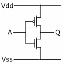
Current MOSFET technology involves, in addition to PMOS and NMOS, the presence of complementary MOSFET (CMOS) circuitry. Even as MOSFETs have come to dominate semiconductor usage in electronic equipment, the CMOS configuration remains the most important design strategy for both digital and analog applications. The reason is that CMOS circuitry involves much less power loss, which equates to less heat dissipation and the accompanying demon of temperature rise. This reduction is made possible by the fact that in CMOS implementation, each NMOS is complemented (hence the name) by a PMOS. Both gates and both drains are connected together. “CMOS” does not refer to an individual semiconductor such as a diode or a JFET, but rather a type of circuitry composed of opposing (and complementary) types of MOSFETs (NMOSes and PMOSes). This circuitry can be constructed as a standalone configuration to illustrate the concept, but the usual deployment is within an IC, where hundreds of millions of these subcircuits can be wired together within a single microchip.
What accounts for the lower power consumption in CMOS technology is the fact that the PMOSes and NMOSes are connected in series. When one is on, the other is off, so the series combination does not draw current, except very briefly during transitions. When great numbers of these CMOS circuits inhabit a small IC package, this minimal heat dissipation is an important advantage and why CMOS circuitry has come to dominate the world of microelectronics.
Information can take either an analog or a digital form. Appropriate electronic circuitry may convert either format to its counterpart. How and where this conversion takes place is critical, and it determines the extent to which CMOS technology is used.
Digital Domination
As we all know, digital equipment has replaced its analog equipment in many areas, such as consumer and professional cameras. However, the image conveyed by radiated or reflected light from the object to be photographed is, for our purposes, an analog phenomenon, notwithstanding quantum revelations.
The light passes through a conventional lens and mechanical shutter, permitting the image to be focused (for a prescribed amount of time) on the sensor. At this point, two divergent technologies have emerged. For many years, the charge-coupled device (CCD) possessed a decisive advantage in quality, but CMOS sensors have improved to the point that they are taking over in key areas. At lower cost and using less power (translating to longer battery life and greater intervals between charges), CMOS sensors have become dominant in both consumer and professional digital cameras, just to mention one venue.
CCD technology involves charge transfer along the array surface between adjacent capacitors. The charge is transmitted across the array, emerging at one corner where an analog-to-digital converter measures the amount of charge and creates binary information in preparation for downloading to the computer. CMOS involves the use of numerous MOSFETs at each pixel to capture the information in preparation for moving it, already digitized, over traditional wiring to the printed circuit board. This is possible, because, as we have seen, there is much less heat to be dissipated in CMOS circuitry, so more devices can inhabit a small chip.
In contrast to the analog/digital camera environment, in strictly digital CMOS technology, inputs and outputs are switched on (1) and off (0) only. If the device is on, it is fully saturated: it is not designed to operate within the lineal portion of its response curve, unlike an analog device. The voltage level (representing 1) has declined. Typically, ground (low voltage) is set at 0 V. In past decades, 1 was defined as +5 volts, but it has since been set progressively lower so that very large-scale integration (VLSI) can be achieved.
CMOS single-stage logic gates are inverting, meaning that when the input is 1, the output is 0, and when the input is 0, the output is 1. To construct a non-inverting device, it is necessary to have multiple (an even number of) stages.
CMOS Troubleshooting and Repair
To design or become proficient in the troubleshooting and repair of CMOS circuits, one must be aware of their steady-state and dynamic electrical behaviors. Parameters are found in manufacturers’ data sheets and include logic voltage levels, DC noise, permissible fan-out, power consumption, electrostatic discharge and tri-state and open-circuit output. For logic 1 to be perceived as an input, the V1H(min) must not drop below the level prescribed by the manufacturer in the data sheet. Similarly, any device will have low-level input voltage, high-level output voltage and low-level output voltage. Aberrations are caused by noise causing unstable circuit operation.
“Fan-out” is a picturesque term that conveys the number of inputs a logic gate can drive without seeing performance degraded. It is a function of output characteristics of the parent device and the number of driven inputs, plus their loading characteristics, specifically their input impedances. Low- and high-state fan-outs are not usually identical, so the worst case is the one that counts. As frequency increases, permissible fan-out becomes more dependent upon the total parallel capacitances, which, of course, are additive. For each CMOS device in the total load, the propagation delay becomes greater, so it is necessary to calculate that amount and compare it to the permissible maximum propagation delay.
If the output is loaded beyond its rating, expect to see the output increase beyond the maximum limit in the low state. In the high state, the output may drop below specifications. Additionally, propagation delay and rise and fall times are likely to go high. Above all, watch out for temperature rise, degrading circuit reliability and, in short order, destroying the CMOS. In the DC state, because of the aforementioned CMOS circuit configuration, power consumption is low. But, as the frequency increases, this advantage goes away. For any given application, it is important to check the manufacturer’s data sheet. The figure rises in large arrays, and it is necessary to ascertain that the supply and conductor sizes are adequate.
A principle area of concern for elevator technicians is the main lift motor. Since speed control and reversibility are always factors, driver issues become prominent. The sole driver can be a MOSFET only in the smallest motors, such as brushless DC and stepper motors. Because they draw more current, larger motors require power semiconductors. In any context, the current-carrying devices must be switched in such a way as to cause the motor to perform as needed.
When referencing the motor’s current requirements, it is always essential to realize that the startup current is greater than the current required for the motor to run at its rated speed, even when fully loaded. This is because when it is not turning, there is no “back electromagnetic field,” and the load is limited only by the ohmic resistance of the motor windings, which is much lower than when the turning armature causes the stator magnetic field to work.
Unexpectedly high voltages can be delivered to the motor windings, causing premature insulation failure under certain conditions. Board and lead inductance can cause ringing in the motor circuit, resulting in unwanted voltage spikes. This phenomenon is more pronounced at high frequencies, but it is important to realize that a fast start and stop time, caused either electronically or mechanically, will do the same thing, even if the basic electrical energy is DC. When repairing, take care in replacing wiring, not to reroute in such a way as to alter the characteristics. It is a good idea to take a look at the waveforms with an oscilloscope while the motor is operating properly so you will know what to expect. Make drawings or, with a digital scope, save the images and keep them on file.
Choosing a Device
The first step in choosing a power-switching device for a motor drive is to consult the motor nameplate in conjunction with the National Electrical Code in order to size out conductors and disconnect and overcurrent protection ratings. Assuming this circuitry is adequate to carry the load, compatible drive ratings can be determined, taking the system voltage, current, phase and frequency into account.
The power-switching device will likely be a MOSFET or an insulated-gate bipolar transistor (IGBT). Recently, the MOSFET and IGBT have replaced the simple bipolar transistor, even in its Darlington form. That is because, while the bipolar transistor is current controlled, the voltage-controlled MOSFET and IGBT are more designer and user friendly. When to use each device is all a question of power consumption and heat loss. The MOSFET is generally used when the system voltage, as delivered to the motor, is less than 250 V. IGBTs are better at more than 1,000 volts. Between these figures, the jurisdictions overlap, so it is best to take a good, hard look at all parameters, de-rating as appropriate.
Conclusion
We have seen that the MOSFET has replaced the once-popular bipolar junction transistor. Special precautions are necessary when handling it to avoid damage from the static charges that may accumulate in the human body or may be conveyed by inadequately grounded electric tools. These devices are also sensitive to heat from a soldering iron, particularly those of the CMOS variety. That being said, these components are user friendly, and, since they draw less current, they have largely replaced earlier solid-state devices.
MOSFETs have made VLSI possible in ICs, and this fact accounts for the feasibility of low-cost computers and all sorts of communication equipment that is so much a part of our lives. From compact cell phones to large elevator arrays that make today’s big cities a reality, the MOSFET plays a key role. For those of us who work on a daily basis with electronic equipment, an understanding of the inner mechanics is a great advantage. One of the keys to this understanding is an ability to access the knowledge as quickly as needed. A great help is the printed word. The cost of one textbook can easily be justified when working on expensive equipment needed immediately. Moreover, a great deal of information is available at no cost on the Internet. The next time you are baffled in the course of a repair, try typing the make and model into a YouTube search bar.
Learning-Reinforcement Questions
Use the below learning-reinforcement questions to study for the Continuing Education Assessment Exam available online at www.elevatorbooks.com or on p. 103 of this issue.
♦ What are the defining characteristics of JFETs and MOSFETs?
♦ Why are extraordinary precautions needed in handling MOSFETs?
♦ How does a grounding bracelet work?
♦ Why has the MOSFET become a dominant semiconductor technology?
♦ What is the advantage of the CMOS configuration?

Get more of Elevator World. Sign up for our free e-newsletter.


