What Is a Transistor?
Dec 1, 2014

Another major electronic component used in elevators is detailed.
Like diodes, transistors are major players in the electronics arena, notably in elevator motion controllers and variable-frequency drives (VFDs) that have an extensive operator’s interface. Also like diodes, the transistor semiconductor mechanism is very simple in that it involves the attraction and repulsion of charge carriers by the bias voltages applied to the device terminals. The electrons and holes migrate toward or away from the semiconductor junctions, thereby regulating higher flows of current between various terminals and ground.
Learning Objectives
After reading this article, you should have learned about:
♦ How transistors operate by attracting and repelling charge carriers
♦ The effect of doping on crystalline silicon
♦ Why the doping process is used
♦ How base, collector and emitter are connected in electronic circuits
♦ How to handle transistors
The defining difference between diodes and transistors is that in the diode there are two layers (N- and P-type silicon, with a single junction between them) where the semiconductor action takes place. This article assumes the reader has already understood the author’s piece “What Is a Diode?” (ELEVATOR WORLD, August 2014) or understands how these devices work on a subatomic level and in electrical circuits. Compared to diodes, transistors are somewhat more complex, because they have three semiconductor layers with two junctions. The materials (N- and P-type silicon) are created essentially as they are for diodes, by a process known as doping. Crystalline silicon is not electrically conductive. (Other semiconducting materials have been used, but today the choice is usually silicon.) But, when it is exposed to trace amounts of certain other elements, the crystalline silicon becomes a semiconductor. This does not mean it has a fixed resistance that lies somewhere between that of an insulator like glass and a conductor like copper. To the contrary, it means that under some conditions, the crystalline silicon conducts, and under other conditions, it does not conduct.
What underlies all of this is that silicon, with an atomic number of 14, consists of a nucleus with four electrons orbiting in its valence (outer) shell. (The number of electrons in the valence shell of any element accounts for its physical properties and the ways in which it interacts with other nearby atoms.) Atoms are able to share valence electrons with adjacent atoms. Because it has four electrons in its valence shell, pure silicon likes to assume the form of a crystal lattice, each atom sharing electrons and, hence, tightly bonded to four adjacent silicon atoms. The crystalline silicon is very stable, and, electrically, it is an insulator.
When the crystalline silicon is doped with phosphorous or arsenic (don’t worry, the amount is infinitesimal), each of which has five electrons in its outer shell, the situation changes abruptly. There is then one free electron for each doped silicon atom. The excess free electrons travel in the spaces between the silicon atoms, and they are known as “charge carriers.” Crystalline silicon, doped with phosphorous or arsenic and thus having free electrons, is N-type silicon. It is no longer an insulator but is capable of conducting an electrical current, due to the presence of charge carriers.
Even when the transistor terminals are not labeled, it is possible to identify them and ascertain the transistor type by looking at the arrowhead.
In a mirror-image process that reverses the polarities, crystalline silicon can be doped by exposing it (so that minute amounts are absorbed) to boron or gallium, both of which have three electrons in the outer shell. This process creates a deficiency of electrons in the space between the silicon atoms. These empty spots are called “holes” and may be thought of as positively charged particles with negligible mass, like protons that have positive polarity but are far more massive. Whether these holes actually exist as particles or more nearly resemble conceptual entities, we can leave to the metaphysicians. The fact is that they are effective as charge carriers and necessary for semiconductor operation.
Crystalline silicon doped with boron or gallium becomes P-type silicon. We have seen in the previous article on diodes that N- and P-type silicon bonded together make a junction. With leads attached at the far ends, they constitute a useful device that conducts or does not conduct, depending upon the biasing.
Transistors also make use of the semiconducting properties exhibited by N- and P-type crystalline silicon. Today, bipolar transistors have been largely supplanted, first by field-effect transistors (FETs) and, finally, by the ubiquitous metal-oxide semiconductor FET (MOSFET), which has much higher input impedances. Nevertheless, there are plenty of bipolar transistors around in older equipment, as well as in contemporary applications. In this piece, we will stick to bipolar transistors, since they are more basic and provide a good background for understanding the more exotic varieties.
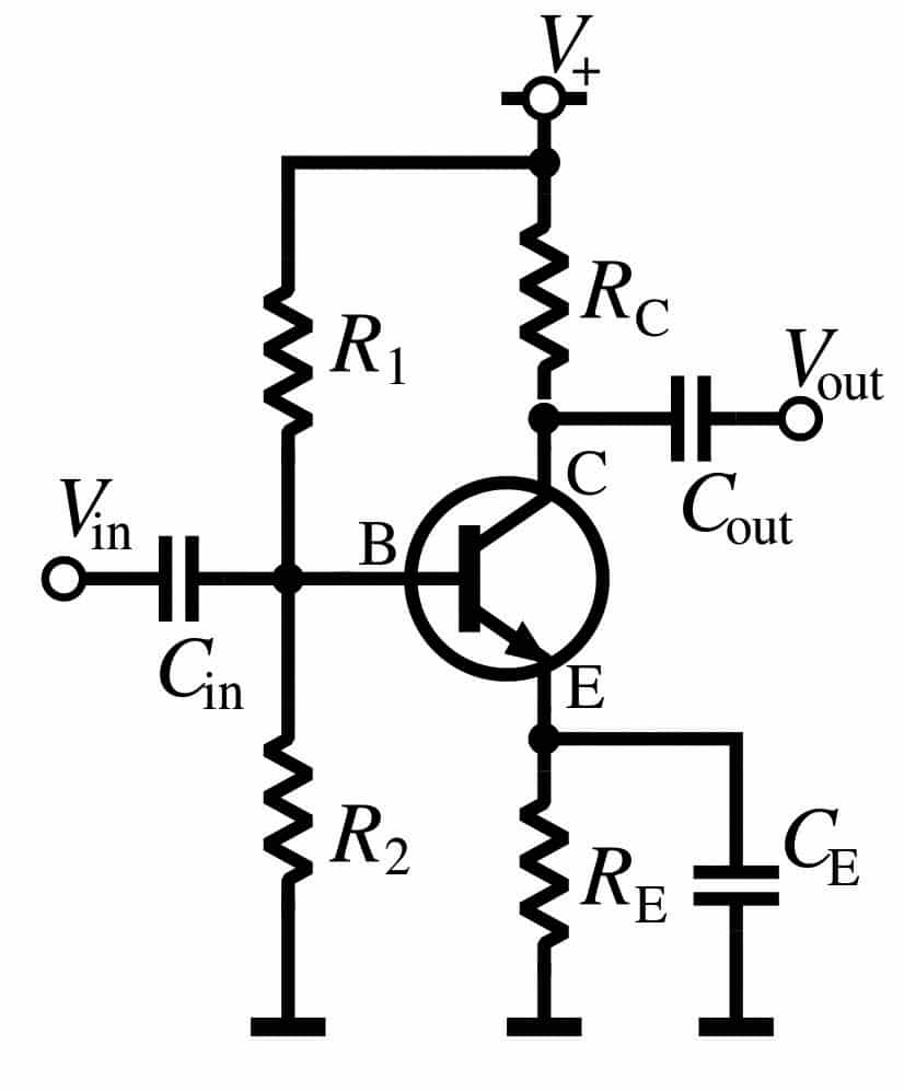
As mentioned above, transistors consist of three semiconductor layers, a base, an emitter and a collector. These terms do not have to be taken too seriously, because the “base” is not a base, the “emitter” does not emit anything, and the “collector” does not collect anything. Still, that is the terminology, and it is quite graphic.
Each layer has a lead attached so the transistor can be wired to other components, such as resistors, capacitors and coils, to comprise a circuit. The three semiconductors are bonded, always with the base in the middle and the emitter and collector on either side. But, do not conclude that the middle lead goes to the base, because this is not always the case. Since there are three layers, there are two junctions. The base has two junctions, and the emitter and collector each have a single junction they share with the base. The emitter and collector have no common junction and are not electrically connected, except through the base and, in some configurations, through external circuitry.
Each of these semiconductors can be P- or N-type silicon. The emitter and collector are always the same type, and the base is the other type. Accordingly, transistors may be either PNP or NPN. The PNP version has an N-type silicon base with emitter and collector composed of P-type silicon. “NPN” indicates a P-type base and an N-type collector and emitter. The two junctions, like the single junction of a diode, may be forward or reverse biased, and so, will conduct or not conduct. In most circuits, NPN and PNP transistors can be interchanged, but all polarities (including those provided by the power supply) will be reversed.
A transistor schematic consists of a circle with an internal semiconductor shown, including leads that permit circuit connections. The base resembles a flat plate like the cathode of a diode. Collector and emitter are lines that connect to the base at an angle. By convention, the base is shown at left, the collector at top and emitter at bottom, but this may vary if required by the overall schematic layout.
The base, collector and emitter may be labeled on the schematic, but not always. You can always distinguish emitter and collector, because the angle line having the arrowhead is always the emitter. Moreover, if the arrow points inward toward the base, the transistor is PNP, and if it points outward, the transistor is NPN. To summarize, even when the transistor terminals are not labeled, it is possible to identify them and ascertain the transistor type by looking at the arrowhead.
Transistors have three leads. With one lead as common, it is possible to have two two-wire circuits, and this is how transistors are configured. The emitter is usually the common connection. In this mode, the base emitter is the input, and the collector emitter is the output. Small input changes result in identical output changes but at a much higher power level. This stepped-up output receives its electrical energy from the power supply, so it is not a question of getting free power. Nevertheless, the input/output ratio makes the devices extremely useful in many types of electronic equipment.
As an amplifier, the transistor can boost an incoming signal applied to the input terminals, so that an amplified version appears at the output terminals. The ratio of base-emitter current to collector-emitter current is known as “gain.” The output of one transistor stage can be coupled to the input of a succeeding stage to achieve greater amplification. A number of stages can be cascaded, so that the very weak signal picked up by the antenna can be amplified sufficiently to drive large speakers, video or other devices. Low-gain transistors have a gain of around 30. A high-gain transistor can reach 800 or more.
As input is increased, the output also increases in a linear fashion. Beyond a certain point, however, the transistor (together with its power supply) is not capable of further amplification and is said to be “saturated.” (This is similar to when an inductor, such as a transformer winding, becomes saturated, and no further increase in electrical current will increase the magnetic flux.) Saturation is not good in an amplifier. The output waveform will be missing its peak levels, with a flat line at the point of saturation. This condition is known as “clipping” and manifests as an unpleasant buzzy component in an audio output.
Besides amplification, transistors may be designed and configured for other purposes. A major use is as an oscillator, which can generate a sine wave or other waveform of any desired frequency. This would apply to a wide range of applications:
- Electronic equipment that incorporates an audio beep such as a telephone, video game or fire-alarm system will have this signal generated within an oscillator circuit.
- A signal generator produces a range of frequencies and waveforms that technicians inject into defective equipment for purposes of signal tracing and viewing (with an oscilloscope) at each stage until the fault is located.
- Clock signals that regulate computers and quartz clocks are generated by oscillators.
- Virtually all radio and TV receivers are superheterodynes. They drop the radio-frequency (RF) signal as picked up by the antenna to a more manageable intermediate frequency (IF) and lower frequencies for successive stages of amplification. The way they do this is by mixing the higher-frequency signal with an oscillator-generated signal so a sum and difference beat signal is synthesized. The desired lower-frequency signal is selected using a simple coil-capacitor resonant circuit. In the early years of radio transmission, the sine wave was generated at the broadcast station and sent along with the programming signal, but today, the tone is locally generated within the receiver. In an old-style receiver, the variable capacitor (which was tuned to different frequencies) was made up of two devices ganged on a common shaft. This was so that, as different stations were acquired, there would be a different oscillator frequency for each so that a single IF could be synthesized for the entire broadcast band.
- A VFD used to provide speed control for an AC motor (such as that in an elevator drive) does so by supplying appropriate frequencies in the power that feeds the motor. These frequencies are supplied by the inverter section of the VFD.
It is possible to get a good idea of the condition of the transistor on a go/no-go basis using just the ohmmeter.
The principle types of electronic oscillators are the linear and non-linear (relaxation) oscillator. A linear oscillator produces a pure sine wave. It consists of a transistor configured as an amplifier with a feedback loop, meaning that the output is connected back to the input. When initially powered up, any small amount of noise generated by atomic motion in the circuitry or within the semiconductor is amplified and conducted back through the input so that continuous amplification and filtering produces the desired tone.
Transistors are purposely operated in the saturated mode in digital circuits, as opposed to the analog circuits discussed previously. They are used in the digital (switch) mode in high-power applications, such as the switching of power supplies, and in low-power modes, such as logic gates. In both designs, the transistor is configured as a switch. It is similar to a light switch (not a dimmer switch) in that it may be either on or off, but not in between. When it is in the cutoff mode, the output is off, and this corresponds to the digital number zero and the logic state “FALSE.” When it is in the saturated mode, the output is on, and this corresponds to the digital number one and the logic state “TRUE.”
A linear power supply, as we saw in the diode article, converts AC utility power to a lower-voltage DC power used in electronic equipment to bias the active components. It performs this task by placing a single power diode in series with one incoming line (half-wave rectifier) or by employing four power diodes in a diamond configuration (full-wave bridge rectifier). Both arrangements are simple and fairly reliable, considering the fact that the power supply is the location where the entire system power flows. The downside is that a substantial amount of power is wasted when dissipated as heat. This is because, for a large portion of the AC cycle, the device is neither turned off (open) nor turned on (conducting all the current); it is somewhere in between. Once again, the Ohm’s Law Wheel is relevant. Power or heat loss is proportional to I2 X R, current squared times resistance. When the rectifier is fully on, R = 0, and when it is fully off, I = 0. In either of these instances, the power wasted, dissipated as heat, is 0.
The switching power supply meets this condition, since it converts the sine-wave input to a square wave with very fast rise and fall times, resulting in minimal heat loss. For this reason, components and the overall device can be downsized, reducing cost and space requirements. There are some tradeoffs, however. First, switching power supplies are more complicated, and more difficult to diagnose and service. Moreover, the high-speed transitions can generate harmful harmonics and RF interference in nearby equipment. Additionally, if there are many of these units in a facility, they may contribute to a poor power factor. Any of these disadvantages may be mitigated by the installation of shielding, judicious placement and isolation from other conductors, and connection to power-factor correction capacitors.
Despite these disadvantages, there has been a major move away from linear and toward switching power supplies, and this is likely to continue. In a switching power supply, voltage regulation is achieved by varying the relative on and off times. The on/off switching action is performed by one or more power transistors operated alternately at below the cutoff and above the saturation levels.
A boost converter consists of an inductor and diode in series between the supply and load. The switching transistor is placed in parallel with the supply and load, after the inductor but before the diode. When off, it is invisible, and when on, it shunts out the diode and load, but not the inductor. The inductor reacts to current changes in the circuit by inducing a counter voltage, which is added to the power-source voltage under open switch conditions. Alternatively, a capacitor can be used in series configuration, creating an output voltage higher than the DC input voltage. In both cases, the switch is a power transistor of appropriate rating.
Failure modes involve shorted or open inductors, capacitors, diodes, transistors, transformers or wiring (including terminations). As always, this equipment can contain hazardous stored voltages that may persist long after the power source is disconnected and locked out. Do not test or service this equipment unless you know the dangers and can safely disconnect it from all sources of power and discharge the stored voltage. A bleeder resistor will perform this task automatically, but nothing should be assumed, because the device may not be properly connected, or it could be open.
A transistor may be tested using the multimeter in ohms mode, the multimeter in diode or transistor test mode, an in-circuit transistor tester, a service-type transistor tester or a laboratory-standard transistor tester. All of these impose a bias voltage as needed. The service-type tester measures beta (forward) gain. It also measures base-collector leakage current with no voltage on the base. Some instruments identify base, emitter and collector leads. The laboratory-standard transistor analyzer applies bias and signal, and reads the output.
An ohmmeter can be used to check a transistor, because the meter’s power supply (intended to provide the current for measuring resistance) is suitable for biasing a semiconductor. To perform the test, the polarity of the ohmmeter probes must be known. Most manufacturers polarize the probes so that black, when plugged into the socket marked common, is negative. But this is not universal, so the best procedure is to check polarity with a known good diode that has the cathode marked with a single band. Then, the probes can be permanently labeled.
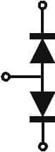
A transistor may be thought of as two diodes with the two anodes (representing NPN) or the two cathodes (representing PNP) connected. This hookup allows for three test points. Figure 3 serves as a learning device to show how to connect an ohmmeter to a transistor for testing purposes, but it will never work as a functioning transistor.
Going back to the transistor to be tested, if you do not have a schematic of the overall equipment, nor a parts number or manufacturer’s data sheet, it is often not possible to know the identity of the three leads and the transistor type. But, using the multimeter in ohms mode, you can bias and measure the continuity of each pair of leads, thereby gathering valuable information.
Each pair of leads can be forward or reverse biased, so there are six possible measurements that can be taken. These measurements provide the only information available from ohmmeter readings. Referring back to the diode model, you will notice that a good diode will read open across two of the leads, regardless of which way the ohmmeter is connected. So, these two leads are collector and emitter, but we do not know which is which. We do, however, know that the remaining lead is the base.
If all three pairs measured both ways read low ohms, the transistor is shorted. If all three pairs measured both ways read high ohms, the transistor is open. Discard it immediately, before it gets mixed into your inventory.
If the transistor passes both of these tests, further investigation is in order. To review, the collector-emitter pair has been identified, and the remaining lead is connected to the base. Connect the probes both ways to each of the other leads. When forward biased, the base will conduct to either of the two leads. The two hookups require different biasing to conduct. From these readings, you can identify the non-base leads if you know the transistor type, or you can ascertain the transistor type if you know the identity of at least one of the leads.
We see that with no information at all about the transistor, it is not possible to determine everything, but with partial information, the transistor type or the collector-emitter identity, we can fill in the remaining unknowns. In any event, it is possible to get a good idea of the condition of the transistor on a go/no-go basis using just the ohmmeter.
Two important attributes of any bipolar transistor are α and β. With base at signal ground, α is the collector current divided by the emitter current, which is the transistor’s dynamic gain. β is the collector current divided by base current when the emitter is at signal ground. These two attributes apply to a transistor wired in two configurations. This relationship is spelled out in the following formulas:
α = β/(1 + β)
β= α/(1 – β)
You can always find α and β in the manufacturer’s data sheets, and these quantities are relevant for design work and for determining a suitable replacement when the original transistor cannot be obtained.
In a circuit board, bad transistors (like other discrete components) can be replaced, but special care is required so they are not damaged by heat from the soldering iron. Attach a heat sink between the component to be soldered and the heat source. Smooth-jawed needle-nose pliers, held closed by means of a rubber band, will work.
(image by Aflafla1).
Learning-Reinforcement Questions
Use the below learning-reinforcement questions to study for the Continuing Education Assessment Exam available online at www.elevatorbooks.com or on p.115 of this issue.
♦ How many semiconducting layers are in the simple transistor?
♦ What causes the resistance of crystalline silicon to change?
♦ Which role do free electrons play in the semiconducting process?
♦ What are the two types of charge carriers?
♦ What are the base, emitter and collector?

Get more of Elevator World. Sign up for our free e-newsletter.